Friday, 19 December 2014

Oak Hills Research OHR WM-2 Watt meter

I'm in the process of building an OHR WM-2 QRP Watt Meter from Marshall Emm's Oak Hills Research (part of Morse Express).


The quality of OHR kits is fantastic, as was demonstrated on their OHR RFL-100 dummy load (see my build here.
I was so impressed that I ordered a few more kits to get into making some more useful and fulfilling projects for ham radio: watt meter, digital counter/frequency display and 20m CW transceiver.

Building up kit-making experience, the dummy load was a very gentle intro to following instructions and soldering. No real challenges there.

Moving onto the WM-2 Watt Meter, the supplied kit is again of very high quality. The aluminum case is robust, light, well-finished and very accurately cut/stamped. Rather than using paint, the facia of the watt meter is a thick plastic sheet with high strength adhesive. No chance of this peeling off with time, as long as you cleaned the aluminum case surface well enough.

What follows is a visual diary of the build. The instructions from OHR are first-rate, very clear, well organised and complete with inventory list of every single part (right down to #4 lock washers,... all my components were in the box without fail) and circuit diagram.


The first component - a resistor

High quality PCB with screen printed component shapes and labels, and solder mask

Diodes go in. The 3 critical germanium diodes are matched for forward voltage bias by OHR. My 3 agreed to within a 2mV error.

ICs are used for the bridge and op amp for the meter needle. They are soldered directly to the PCB without IC holders.

Trimmer pots are added to calibrate and align the meter need full deflection at specific voltages. Three of them are standard kit items, used to adjust the meter need full deflection points. The fourth is used to adjust a voltage drop to an accurate value, down to the millivolt. I have read from other builders that the standard trimmer pot (1 turn) is a bit time consuming to achieve the correct millivolt readings. So, I installed a 25 turn trimmer pot in its place, hoping to control the resistance, and hence required voltage drop, with ease to the required millivolt accuracy. This is seen in the photo above as the blue rectangular item.

My very first hand-wound toroids. I remain uncertain at the time of writing if the coils extend far enough around the toroid ferrites. In this photo they rest at approx 2/3 the circumference. 

Finished toroids and coax cable signal sampling. Together, they form transformers that tap the RF power flowing through the meter. There are two transformers, once for  forward and the other for reverse power. Marshall Emm's technique for tinning the enameled wire works well: apply solder iron tip to heat the end of the wire and apply a glob of solder. Keep the iron in contact and the enameled coating with bubble up through the solder glob. Run the iron down the wire, feeding solder as needed to maintain coverage and bubbling. The wire ends naturally seem to straighten!

First transformer mounted. The toroidal coil coverage is now closer to 270 degrees (3/4s) circumference, since the ends of the wire need to be drawn parallel together to be inserted into the PCB holes. 


The instructions advise to try to make the toroids as nearly identical as possible to tap power in the same way. This removes variation from the comparison of forward vs reverse power measurements.
I may look at increasing the toroidal coil spacing to get the coils to cover more of the cores (say 300 degrees around).


Getting ready to cut and prep the wiring loom

Tinning


The PCB and switches are done. Now for final assemble of the case and hardware.


The workspace. The watt meter is coming along well.

One thought on powering the watt meter. There is no stabilised voltage regulator in the circuit. It is designed to work from an internal 9v PP3 battery or external DC supply from 9v-13v. This wider DC range is only used to power the ICs and meter needle. These op amps have voltage regulators built in, so there should be no need to add an LM7809 for example.


To test the finished meter, I plan to use my Elecraft KX3. This is an SDR digital radio (without the computer) and offers me the best 'reference' on power outputs and SWR via its built-in ATU.
I plan to control the KX3 power output to assist in calibrating the meter once the set up without the rig is done. This will offer me some validation of the WM-2 setup.


Monday, 15 December 2014

Casio SA-65 Part III - fixed it and learned a lot

In my two earlier posts, I described a Casio SA-65 electronic keyboard that appeared to be working (after removing lots of battery compartment corrosion on the negative terminals) except for the annoyance of failing to produce notes correctly on specific pairs of adjacent keys on the piano.
These pairs of keys, spread over each octave of the piano's 37 leys, would sound both pair's notes (e.g. D and D#) when only one of the keys - either one - was pressed.

Opening up the keyboard to investigate, I've spent some hours reviewing the schematics (see Part I for a link to the Casio SA-65 service manual, or just Google for it). My experience of electronics is still very basic, but while I am pleased to state here that the keyboard now works well, I must admit that I've only really overcome the symptoms of the problems and not truly resolved the deeper issues with this keyboard. It can now be used as intended, while inside lurk some glitchy CPU processes!


What bad diode?

My trials and errors in finding a solution to make the Casio work again, led me into a few alley ways and perhaps some crazy conclusions. This is all part of my learning process. One example was my confident assertion that there was a bad diode, D104, on the PCB.

This is flatly untrue! 

Measuring all diodes in circuit, I measured the expected 0.6V forward bias voltage drops and 'OL' reverse bias levels. All except in one place, D104. My inexperience and enthusiasm got the better of me and I wrongly deduced this D104, measuring 0.1V forward and reverse and 100Ohm resistance, was defective. I desoldered it and replaced it with a known good diode: but the original diode measured out of circuit was fine and the good new diode measured in circuit was bad!

I'd misinterpreted and ignored the schematic details (above) and forgot that measuring voltage across D104 would involve all components in parallel with its anode and cathode - like that 100Ohm resistor (see above).

So there were no bad diodes, and my assumed cause of 'ground bounce' was not the source.

There IS ground bounce in the circuit, as seen from a CPU output pin (KO0) and the noise in sync on a quiescent input pini (KI0) that was not affected by the phantom signals:

blue - KO0 output, yellow KI5 input (good signal), purple KI0 input (phantom signal)

Soooo, I know there is some 'bad' effect from the quiescent pin ground noise, but have no idea what is causing it or how to resolve it.

But that does not mean I cannot resolve the issues that make the piano unplayable: the two-tone keys. Looking at the above screenshot as representative of the idea that follows, we can see that the phantom signal is somewhat lower in peak voltage compared to the desired signal.

Using this observation, I added a potentiometer (470KOhm) in series with KI5. The idea is to create a voltage drop across the resistor which will attenuate the signals on pin KI5 - that includes the wanted and unwanted square wave pulses. By finding just the right resistive level (hence the adjustable pot), the wanted signal is above the CPU threshold for a 'high' input, while the unwanted phantom signal is below.

I did this successfully on the affected pins KI5 and KI6 (different resulting resistances were needed) and soldered these new resistances in series with the circuit towards the CPU pins.


The two-tone sounds went away after that, so closed up the keyboard and happily sent this keyboard onwards to new owners.

Thanks for reading.


Friday, 12 December 2014

Casio SA-65 repair.... Part II

Following yesterday's post on the observed issues with a Casio SA-65 electronic keyboard, and my attempts to resolve them, I'm able to make a short post to follow-up on two topic mentioned there: Jitter and Ground Bounce.

CPU output pin jitter  

I remarked that the CPU has output pins that send a square wave pulse out towards the keyboard - the key scan signal. The keyboard switching arrangement is a matrix, and the CPU listens on input pins for a received signal from a closed circuit, i.e. a piano key being depressed.

The CPU decides what note to play based upon a) what input pin has a non-zero signal (since all the input pins are quiescent in the absence of a signal) and b) WHEN that square wave pulse is, relative to the CPU's string of pulses sent from each output pin in turn. Imagine your rolling or wrapping your fingers on a table top as you wait impatiently for waiter service to ask for the cheque. Your fingers sequentially tap the table, say little finger first, then ring finger, then middle finger, fore finger and lastly thumb, then back to the pinky finger again....This is the CPU firing pulses at the outputs and where a pulse is, relative to some internal counting or reference pulse, is information used to define the output pin used (see the last post for a picture from the service manual on this point).


I had commented that the KO0 output was jittery,
and last night was able to take a look at that jitter. The screenshot below is a trace of KO0 from my Casio SA-65 CPU. The trace as a static picture is misleading as it suggests uniform periodicity.


In actual fact, the pulses are a bit all over the place. Below is a screenshot showing the blue KO0 pulses, but as an envelope trace: rather than a single sweep and trace as above, we see multiple sweep traces laid on top of each other - in an analogue oscilloscope, you would get the same effect my increasing the phosphorous persistence rate and let all earlier traces linger on the screen for longer:


Clearly, the KO0 pulses are actually mis-spaced to the extent that the CPU listening to this signal would easily create false key notes by thinking that outputs other than KO0 were connected via piano key pressing.

This jitter supports the analysis made in my last post to explain the many octave notes that lurk in the speaker output, but which are not sent to the CPU pin because of the bypass capacitors connected to ground at the input pins. Increasing the capacitor size, smooths these mixed pulses across wider 'pulse time slots' and allows the CPU to 'see them', and musical notes result.

Ground Bounce

The jitter resolved above is a digression, since it does not answer the reason why the jitter exists in the first place. One idea was the existing bad diode in the power supply circuit, D104.

This bad diode would possibly create problems with CPU oscillations and result in the jitter confirmed above, and also might have a role to play in any ground bounce. 

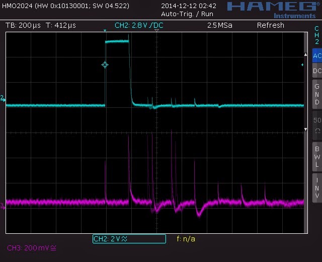
With limited time last night, I was able to look for ground bounce on quiet pins of the CPU. I started by looking at KO0 output pulses (blue) and a KI5 input pin (yellow), which are linked in a closed circuit when depressing the lower D piano key. We see the expected KO0 signal appearing as a copy at KI5 (see below screenshot). However, I monitored an unused input pin, KI0 (purple):


Expectation would suggest the quiet input pin is near 0V, but we see a distinct pulse in sync with the pressed key (KO0&KI5). This is a phantom signal. Indeed, if the peak voltage were higher (it is just over 2V in the trace, compared to 5V for the real signal), we might hear the phantom note at the speaker.

Clearly, the device ground of quiet pins is not so quiet.

Zooming in on the same quiescent input pin, KI0, where there is no piano key depressed, we see that each output pin pulse (using our KO0 in blue trace), we see there are indeed ripples and bouncing when there is a high/low or low/high event. In the shot below, KO0 (blue) fires a 5V square wave pulse. At the same moment, KI0 (purple) feels spikes and ripples in what is technically the CPU ground state:

KO0 (blue) 2V per division. KI0 (purple) 200mV per division

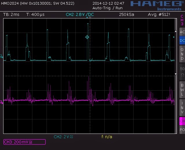
An alternative view of the same event, this time averaged over 512 samples. Since the CPU output pulses for each pin are around 350Hz, this sample of 512 gives an idea of the typical 1.5 seconds of output pin behaviour. We can see dramatically that instead of regimented square wave pulses, the KO0 trace looks like the Manhattan skyline, while the ground bounce is very messy at each square wave event.


In summary, the noisy 'device ground' and output pulse jitter suggest strongly a problem of timing in the CPU and clean ground bias. As was seen in earlier in this blog, even unrelated input pins like KI0 can appear to have significant square wave signals that might be interpreted as key strokes on the piano. [Note: KI0 is physically furthest from the KI5 pin I have studied, yet still carries a 2V peak pulse. KI6, which does yield audible note production (it has nearly 5v peak signals (see last post picture) is next to KI5. Perhaps physical proximity of pins on the CPU is the reason why KI6 is heard with KI5, given some initial biasing that the other pins do not have.... KI5 and KI6 are furthest from the CPU ground pin, for example....].

That bad diode D104 is the next task to try to repair this electronic keyboard.   


Thursday, 11 December 2014

Trying to repair a Casio SA-65 electronic keyboard.....car boot sale special for £3

The other day, my household came into the possession of  a car boot sale 'bargain' for £3 of a 37-key Casio SA-65 electronic keyboard.

It suffered from a badly corroded battery compartment (actually, the compartment lid is missing and tape was used to hold the 5 x AA for 7.5V supply). The accompanying AC/DC UK wall wart power adapter was a generic Goodman 12V 1.5A device, not exactly a good match.

I re-purposed the AC/DC wall wart for a power supply on my recent Almost All Digital Electronics 10MHz frequency standard (see other posting) and set to work to try and clear the battery compartment of the Casio.

I opened the keyboard up. Here and there was a fishy-smelling brown goop on battery connectors, some through-hole components and casing. Using Naptha as a cleaner, I quickly removed the goop and assessed that the negative battery connector was heavily clogged with a the insides of along-dead AA battery. I desoldered the negative connector and plunged it into a home-made mix of corrosion fighting soups:


  1. one tablespoon of table salt in a small glass, and diluted with vinegar (I only had sherry vinegar, so my photo is a darker red-brown - that is the vinegar, not any corrosion!)
  2. a stop-bath of one tablespoon of sodium bicarbonate in water to halt the acid bath
I let the wire steep overnight (6 hours in my house if I am lucky!) in the acid, the plunged it in the base to stop and used a wire brush to remove what remained. The resulting wire is heavily pitted, but conducts well.


With power restored via a bench DC supply, I then discovered the reason that the keyboard was probably left derelict and worthy of a car boot sale: not all keys worked as they should.

Every octave, two adjacent keys are inexplicably tied together: press lower D and you hear D & D#. Press D# and you hear D and D#. Ditto for higher pitch pairs: A# and B, F# and G, then higher still D and D#, A# and B. All other keys are fine.

I was lucky to find the service manual online for the Casio SA-65 here and started my analysis.

The keyboard matrix plan shows that KI5 and KI6 (two of the 8 CPU input pins) connect all the keys above to the 5 CPU output pins (KO0, ..., KO4) that are used to record a musical keystroke (other outputs and input pins record menu select buttons, volume, etc.)

So, why is a note pressed on KO0&KI5 causing the CPU to think KO0&KI6 are connected too (and vice versa, and ditto for KO1, 2, 3 and 4 with these inputs)?

The problem is not in the keyboard nor 'ghosting' that occurs a) when 3 of 4 adjacent keys in the keyboard matrix are pressed, while b) all diodes are 'broken' or not installed (a great explanation is found over at this site : basically my issue does not fulfill the conditions required for ghosting: all anti-ghosting diodes are in place and working and I am not pressing 3 keys).

Indeed, I desoldered the KI6 cable on the PCB board to establish that the unwanted image of KO0&KI5 that appears on KI6 is NOT coming from the keyboard: with KI6 at the keyboard disconnected from the main PCB, the KI6 was still reaching the CPU.  There are no shorts across KI5 and KI6 on the keyboard itself and all diodes are fine. The issue lies on the main PCB somewhere.


Looking at the schematic (see service manual), the only other locations where KI5 and KI6 'get close' is at the CPU. I desoldered the KI6 pin resistor (R127) and still the problem occurs of two notes when KO0&KI5 is closed (lower key D on left side of keyboard).


This places the issue much closer to the CPU itself, or the bypass capacitor that is formed by a 'module capacitor' of 7 0.1nF caps with common ground pin (you can see this from the description as MC101 CNB7x101K = 7  '101' (0.1nF) caps of K tolerance (10%)).

Trial and lots of error

Starting to scratch my head, I am currently exploring two possibilities:
  1. Ground Bounce
  2. Bad bypass capacitor
The idea of 2) is based on some uninformed observations (!) by me:
If you ground CPU input KI6, the image note (D#) of KO0&KI5 (D) goes away (yes!), but then no note from KO0&KI6 (D#) occurs since any signal is taken to ground and away from the CPU.

While playing with extra caps in parallel to the on-board caps noted above, I observed that using a KI6 in series with a 10nF cap connected to ground (this cap is then parallel to the on-board 0.1nF cap, and adds capacitance to the bypass circuit) restored the image note (no more DC grounding at pin KI6) but also created a THIRD note (for one keyboard key press) that sounds an octave higher.
Increase that series cap to 100nF and FOUR notes are heard.... what is going on?

My thinking here has something to do with how the CPU sends out a pulse wave to each output pin. The photo below shows the KO0 pulse output signal from the CPU: 5V pulse, around 350Hz.  However, this pulse is not steady and has some jitter, if I judge by the flickering screen on my 'scope.


This jitter means that within each second, there will be pulses a but later (or earlier) that the rising edge of a true steady square wave. The CPU however differentiates an output pin by the relative timing of the pulses, as summarised in the service manual diagram here:

This means the 'key scan signal' on KO0 can be misinterpreted as another output pulse if the square wave is seen at a different time: it might look like a KO1 pin pulse for example (see above image).
This would mean that a KO0&KI5 key press (D) creates a circuit that contains a false KO1 signal, which - according to the keyboard matrix table - is is KO1&KI5 key press = A# (8 notes higher). Presumably, KO2, KO3 and other false pulses will be sent to the CPU on the KI5 input pin, so why are these not heard?

The answer seems to be the amount of capacitance at the bypass to ground. As noted, adding 10nF bypass cap 'reveals' a third note, and making that a 100nF cap reveals a FOURTH note even higher up (which supports the idea of lots of false signals at KI5).

I have not tested all output pins for jitter (I might as well have a look). Perhaps it is not there, hence the reason why the other keys work well.....

The larger bypass capacitance may be explained by its smoothing effect: think of the input pin receiving several square wave pulses out of sync, faking the multiple key presses, which is smoothed to ground. Square waves convert to a sort of triangle/ramp waves when run though bypass caps (Wiki link for this diagram:


The larger the cap the more spread out the original pulse width becomes since the small caps discharge quicker (so the curved shoulder and toe in the blue line is steeper in transition and appears closer to a square wave). This capacitor spreading affect and the closely spaced/adjacent pulses from output jitter would mean the CPU 'see' significant voltages across the timing of rising edges, which it interprets as many keys pressed, so makes those notes at the speaker.

All that aside, this does not help to understand the reason for a KI6 signal on a KI5 input to the CPU.

The on-board capacitor may be faulty and I am will try to measure it for behaviour

Lastly, the other way to possibly create an issue is Ground Bounce.
This is described here in a downloaded ppt. The summary seems to be this: 

The 'device ground' of a quiescent pin on an IC can be different to the 'electrical ground' of the circuit. Ideally, when a pin is low, it should be 0V in line with the electrical ground. But it seems there are instances where transitions of low/high or high/low voltages , which create current changes (di/dt) can combine, with inherent circuit inductance, induced voltages that move relative voltage levels. In some sense, 0V in an IC can detach from 0V at the power supply. This can pre-load a pin voltage at an IC to be higher or closer to a TTL logic threshold and create phantom signals.

I need to measure a quiet input and output pin on the CPU compared to a high/low or low/high input to see if there is a ripple or bounce in 'device ground'.


There is a broken diode on the PCB board, D104, that shows only a 0.1V forward voltage (not the expected 0.61V for this type of diode) and 0.1V in reverse voltage  - this is a significant failing of a diode. This diode exists in the power supply circuit and allows a circuit to exist between analogue ground (AGND) and digital voltage (VDD). Perhaps this allows a ground bounce effect to affect digital signal levels? The analogue ground is related to a transistor pre-amplifier that smooths the CPU waveform into an analogue sine wave, passing it to a 1W power amplifier chip. 
Also, looking at the schematic, there bad diode D104 could affect the CPU oscillator (21.725MHz) which might explain the jitter on CPU output timing mentioned above.

I will replace the diode and observe the results.


This is a work in progress, so watch out for a new posting about the next steps.

Thanks for reading.


Tuesday, 2 December 2014

Almost All Digital Electronics (AADE) 10MHz frequency standard review

I've purchased this 10MHz frequency standard to assist me in aligning an amateur radio transceiver kit that I plan to build in the coming months.

This device does a simple job: produce a stable and accurate known RF output. I purchased this for $55 (approximately £35), plus postage and handling from Milestone Technologies (aka Marshall Emm N1FN, owner of Oak Hills Research and other ham radio-oriented businesses in Aurora, Colorado, USA). AADE is a separate business run by Neil Hecht and Milestone Technologies is a reseller of some of their products.

The AADE RF standard is a TCXO operating from a regulated 5V supply (via an 7805-type regulator) and producing a 10MHz, with a cascade of decade dividers  (i.e. IC chips that divide the frequency by 10) to allow switchable outputs of 10MHz, 1Mhz, 100KHz, 10KHz, 1KHz, 100Hz and 10Hz and 1Hz outputs. The 5V signal is passed to the BNC female output plug via a 51Ohm-510Ohm voltage divider to yield a 0.5Vpp square wave signal.

The box was well packed with styrofoam 'peanuts', coming with the RF standard (ready-made), hard plastic box, some fixing self-taping screws to secure the top plate to the box and a 1-page instruction sheet, which includes a circuit diagram.

The instructions explain that the connected 9V (PP3) battery connector is part of the testing and alignment process. The RF standard is not intended for battery operation and owners should supply their own wall wart DC or AC power supplies, soldering the cables to the PCB board marked - and +. The RF standard can use 6-18V DC or 6-12V AC.

I desoldered the 9V battery connector and reused a car boot sale-salvaged 12V DC 1.5A wall wart (UK plug type) to good effect. [Yes, I tested the wall wart to check it worked and validate the output of 12.28V DC, within 2.5% of spec].

 To do this, I drilled the case to create one hole to allow the cable into the case, using a 12mm cable gland to tighten down on the cable and prevent any pulled cable from tugging on the soldered ends/PCB board. I also added an underwriters knot (i.e. electricians knot) to ensure tug-free use.


Once sealed up, I tried to measure the output. AADE states two things in the instruction sheet:

  1. Examples of this device have been calibrated against rubidium standards to 0.1ppm accuracy (1Hz error at 10MHz).
  2. Neil Hecht of AADE has no long term experience of how these products age. However, he does note that the same TCXO is used in a number of his frequency counters and drift is very low (he comments of one example recalibrated after only 7 Hz drift in 6 years).
With access to an oscilloscope, I did some quick tests to gauge how true the outputs were at various frequencies. My oscilloscope is not intended as a frequency counter itself, offering 50ppm error according to its specifications.

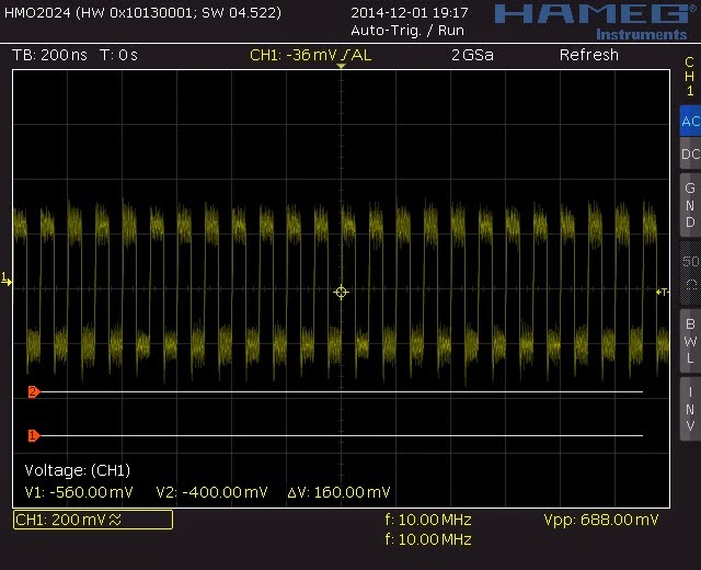
Below are some screenshots from the 'scope, showing RF standard outputs at 10MHz, 100KHz and 1Kz respectively. Frequency counted is shown below the waveforms and suggests the RF standard is 'close' to the target outputs.
You can see the square wave output is rather rough in output with ringing and harmonics distorting the shape. However, this device is not intended as a signal generator, but purely as a stable and accurate 'metronome' at RF frequencies.


My next test was with a ham radio rig: using my Elecraft KX3, I positioned the RF standard close to the antenna socket of the rig, but not connected (no coax, no wires).  I expected there to be enough power and proximity for the sensitive receiver section to 'hear' the RF standard output.

Using SSB on USB, I started just above 10MHz and listened in headphones to the beat frequency generated in the receiver between the rig's VFO setting (10,001,000 Hz) and the RF standard output (selecting 10Mhz on the switch). As the two frequencies differ by less and less, the difference becomes low enough to fall into audible range (e.g. 1000Hz, 800 Hz, etc...). By dialing the VFO closer to 10MHz on the rig, I heard the audio tone lower and lower until at 10,000,070Hz I heard nothing more, as the tone went too low for my ears.

I repeated this exercise in LSB and starting below the target, at say 9,999,000 Hz, I heard the audio tone descending as I increased the VFO until 9,999,930Hz when the tone was too low for my hearing.

This holistic analysis suggests the RF standard output for 10Mhz is indeed within 70Hz of target, i.e. 7ppm error. That is incredible for a simple circuit and matching low cost of £35! 

The low cost is apparent in the paper facia stuck on the box top rather than something made of plastic, while the PCB with through-hole plating is effective, but not far from home-made etching standards. My version appears to have some soldering iron touches to the DC supply ripple electrolytic capacitor's casing: a few melted contact areas. 

Overall, I do recommend this product as a simple and effective and apparently accurate (<10ppm) RF standard that is very portable (light and compact) and does one job quite well.


Friday, 14 November 2014

Oak Hills Research OHR RFL-100 dummy load review

Hi all,

This is a simple blog to document some ham radio kit building experiences I'm gaining. I have no commercial or private connection to Oak Hills Research. I am solely commenting as a customer of this product and sharing my personal opinion. I purchased my kit at full list price and have received no preferential terms.

First blog is the OHR RFL-100 dummy load, a 100W (continuous) 50Ohm non-transmitting load for amateur radio transmitters.

I was unclear on how such dummy loads actually work, since if you search for these things on the internet you often see images of black, finned sci-fi devices or painters tins filled with oils or others that appear as metal bricks. After this kit, the concept and simplicity of these important devices is clear.

This kit from Oak Hills Research is a make-it-yourself item and is extremely easy to build - I finished mine in 1 1/2hrs, including coffee breaks! The quality of the crisp PCB, the weighty resistors, the excellent fit and finish of the all-metal case (expoxy and crinkle paint finished) and hardware were a joy to hold and behold.

I was so impressed with the invested attention to detail from Marshall Emm's (N1FN) company, that I've ordered more OHR kits to build, learn from and enjoy. I'll be adding to this blog as a record of those experiences.

In the end, my dummy load from OHR measured a final impedance (as presented at the SO235 socket) 49.7Ohm - a deviation of just 0.6% from perfection and well within the tolerances of 50Ohm +/-2% stated in the kit's instructions.

Since most rigs have a 50Ohm output impedance, they operate as intended when ideally connected to a 50Ohm load (max power transfer theorem!). Hence, these dummy loads should appear as 50Ohm.

From my measurements with a RigExpert antenna analyser the SWR measured from the OHR RFL-100 was noted as :
  • 80m, SWR = 1.00
  • 40m, SWR = 1.00
  • 20m, SWR = 1.00
  • 15m, SWR = 1.01
  • 10m, SWR = 1.02
  • 2m, SWR = 1.38
These are fantastic SWR ratios, given the load is from a kit and priced at $40 or so. Great value and by far equal to any commercial units available.

I present the build in a series of photos below:


Above: the return path of the RF circuit uses the aluminum case. So a metal to metal contact is needed between the SO235 mounting bolts and the chassis. To remove the quality paint job within the holes, I rubbed the holes out with a undersized drill bit to good effect.